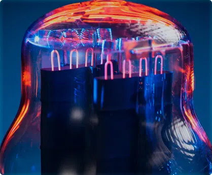
Adgex AIDELab
is a structural division of ADGEX LTD Company, developing state-of-the-art solutions in the domains of electronics and material engineering. AIDELab represents a modern center of unique competencies, encapsulating several key technologies in the fields of single crystals growth and the newest intellectual microelectronics.

Project Manager

Vladimir Zasemkov
Dr. Zasemkov is a founder of modern vacuum electronics in microelectronic field, capable of creating a whole new generation of the electronics. Previously Dr. Zasemkov held senior positions in various international companies, including SI Diamond Technology Inc. in Austin, Tx, USA. Since 1989 he has headed the laboratory of "Vacuum microelectronics".

История AIDELab

1986

Development of the design and manufacturing technology of an autoemission cathode on a silicon substrate

1988

Development of a planar-end topology cell on a dielectric substrate using VLS technology

1990

Manufacturing the world's first experimental samples of cathodoluminescent displays using VLS technology

December 1990

Creation of the vacuum microelectronics laboratory

October 1992

Presentation of the world's first prototype of a cathodoluminescent display to the global community

February 1993

Joint testing of the cathodoluminescent display at MNIITI (Moscow Scientific Research Institute of Television)

1993

Comprehensive patenting of VLS technology

July 1993

Presentation of the world's first cathodoluminescent display prototype at the international conference on vacuum microelectronics in the USA (6th IHT Vacuum Microel. Conf., Newport, Rhode Island, USA)

1993 - 1996

Conducting joint work on the creation of a field emission display with SI-diamond technology (Austin, Texas, USA)

1998

Manufacturing an improved second-generation mini-display prototype using VLS technology

2001

Development of the design and technological basis for creating vacuum integrated circuits (VLS). Patenting new developments in VLS technology

2010

Development of the design and technological basis, creation of a new electronic component base (ECB) for VLS

2012

Development of the concept of the AIDELab neuromorphic chip

October

Start of the concept and design development of the first atmospheric growth chamber for the method of synthesizing 'ideal' crystals

December

Victory of the 'AIDELab Neuromorphic Chip' project at the 'MORE THAN MOORE' innovative IT projects competition (SKOLKOVO-FPI, Russia) in the 'high-speed computing' category

2015

Development of the concept of a terahertz transceiver chip for the Internet of Things. Development of a cathodoluminescent lamp prototype for highly economical lighting systems

January

Start of production of the first atmospheric growth chamber for the method of synthesizing 'ideal' crystals

May

Presentation of the 'Cathodoluminescent lamp with controllable brightness' and 'Terahertz transceiver' projects at the 'Modern Electronics Problems' conference in Krasnoyarsk, Russia

September

Presentation of the design and technological basis of the new VLS ECB, based on ballistic transport of charge carriers at the 'Microelectronics 2016' International Forum in Alushta, Russia

September

Presentation of the 'Development of a transceiver for the Internet of Things' project at the 'Innovation Festival' microelectronics startup competition in Alushta, Russia

October

Analysis of the development of modern microelectronics manufacturing worldwide, identification of new trends and tendencies. Building the AIDELab business concept and business model in the AIDL format

March

Launch and testing of the first atmospheric growth chamber. Confirmation of the functionality of the 'ideal' crystal synthesis method

August

Official start of the AIDELab project

August

Signing of a Memorandum of Cooperation with TOKYO BOEKI GROUP and YOKOGAWA (Japan) and contracts for the supply of the first minimalFAB complexes in the world

September

Creation of our own Design Center as part of the AIDL AIDELab format implementation

January

Allocation of working capital

January

Purchase of components and production of 11 growth chambers for the crystal synthesis section as part of the launch of the first AIDL AIDELab laboratory

February

Acquisition of crucibles

March

Creation of a site for crystal processing and auxiliary equipment

May

Creation of an electronic laboratory for maintenance and repair of growth installations

June

Development of project documentation

June

Purchase of components and materials for the creation of the first AIDL AIDELab format laboratory

September

Creation of an electronic laboratory as part of the launch of the first AIDL AIDELab format laboratory

December

Opening of the second Design Center for engineering of instrument-making production as part of the launch of the first AIDL AIDELab laboratory