Agile
Integrated
Device
Laboratory

AIDL is the newest technological model, making the electronics "individual" and reducing the huge areas of modern production facilities to the size of small mini-laboratories. VITIM has divided all key intellectual and production chains of modern microelectronics, carried out full reengineering and converted each of the processes into the format of space-saving production unit. AIDL approach encapsulates engineering and scientific center, synthesis of ideal crystals technology and mobile modular production of highly-integrated microcircuits, "system-on-chip" and "system-on-crystal"

New Format of Microelectronics

AIDL format stands for Agile Integrated Device Laboratory and represents a brand-new technological format, which transforms current patterns in microelectronics into "individual" approach, reducing the huge areas of the present-day production facilities to the size of space-saving mini-laboratory.
AIDL Format Flowchart
Design & Adaptation of IP Modules

Design of IP-modules based on structural and technological basis of vacuum and combined electronics (vacuum + semiconductor electronics)

Re-engineering of IP-modules

Engineering Center

Structural and technological development of microchips

IP-tuning & re-engineering of microchips

Production of fully-featured superior devices SiP (System-in-Package), SoC (System-on-Chip)

Neuromorphic systems of artificial intelligence (AI)

Foundry – Chip Production

Foundry – tailored approach in chip production

Replication of own products

Production of experimental and pre-production batches

Laboratory tests

Distribution

Comprehensive operation-wise delivery and sale of minimalFAB units to end customer with all pertinent component parts and consumables (within the region);

Commercialization and delivery of the technologies (synthesis of crystals, integrated turnkey production technologies)

«FOUNDRY», but not a «FAB»
Mobile Microelectronic Production

AIDL approach integrates scientific and engineering centers, design-center, single crystal growth and processing areas, and flexible production line of SoC (System-on-crystal) and SiC (System-in-Package).

minimalFAB is a set of space-saving high-tech units of 30cm in width, capable of processing wafers with diameter of 0.5 inches and producing various chips in small and medium numbers. Each technological process of a chip production is fulfilled using different minimalFAB unit. Processing time of a wafer on a single minimalFAB unit takes no more than 60 secs. The units are interconnected with robot manipulator, which carries out transportation of wafers in hermetic containers "Minimal Shuttle". The shuttle obviates the need for sterile rooms, expedites overall production process, and significantly reduces the expenses.

Mobile production laboratory of AIDL VITIM allows producing microelectronic tools on Si, Ge, GaAs, SiN, SiC substrates under the technology CMOS, CMOP, MEMS, NEMS, VIS and other advanced fields of electronics development.
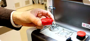
"MNIMAL SHUTTLE" CONTAINER
The method of a maskless lithography is used in the technology of minimalFAB units.
Waffle transportation is carried out in individual hermetic containers "Minimal Shuttle"
No need to make artwork masks or equip the lab with sterile room. This shortens the preparation time for production process, reduces operational costs and makes it possible to responsively change the product’s topology.
Competitive Advantages of AIDL Foundry
  • Tailored approach
  • Any batch to order
  • Short production time
  • Low production cost
"Minimal Shuttle" Container
The method of a maskless lithography is used in the technology of minimalFAB units.
Waffle transportation is carried out in individual hermetic containers "Minimal Shuttle"
No need to make artwork masks or equip the lab with sterile room. This shortens the preparation time for production process, reduces operational costs and makes it possible to responsively change the product’s topology.
minimalFAB Operation Principle
Technological process of chips production includes the units of primary processing, wafers control, photolithographic cluster, the units for dry and wet etching of thin films, thermal treatment, a set of units for metrological control and packaging of readymade microchips under the "flip-chip".
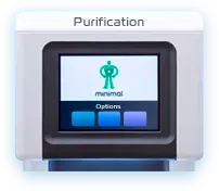
Cleaning
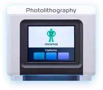
Photolithography
Etching and Oxidation
Packaging
Readymade Microcircuit
The process implies cleaning of wafers using organic solvents in alkaline or acid mediums.
Lithography includes preliminary liquid cleaning of a wafer, photoresist coating, maskless exposure, plasm etching and photoresist removal.
Exposure to high-temperature laser, infrared, and thermal processes in a vacuum and under pressure.
The final stage of microelectronic production, when semi-conductor crystal is packaged.
Cleaning
The process implies cleaning of wafers using organic solvents in alkaline or acid mediums.
Photolithography
Lithography includes preliminary liquid cleaning of a wafer, photoresist coating, maskless exposure, plasm etching and photoresist removal.
Etching and Oxidation
Exposure to high-temperature laser, infrared, and thermal processes in a vacuum and under pressure.
Packaging
The final stage of microelectronic production, when semi-conductor crystal is packaged.
Readymade Microcircuit