El enfoque AIDL combina centros de investigación e ingeniería, centro de diseño, crecimiento y procesamiento de cristales de alta calidad y una línea de producción flexible para fabricar chips para "sistemas-en-chip" y "sistemas-en-paquete".
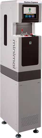
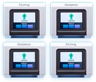
minimalFab es un complejo de instalaciones tecnológicas compactas de 30 centímetros de ancho que permiten procesar sustratos de 0,5 pulgadas de diámetro y producir rápidamente varios chips en pequeños lotes. Cada proceso tecnológico de fabricación de chips se implementa en una instalación minimalFab separada. El tiempo de procesamiento de un sustrato en una instalación no supera los 60 segundos. Las instalaciones están conectadas entre sí por un manipulador robótico que transporta las placas en contenedores herméticos "Minimal Shuttle". Minimal Shuttle elimina la necesidad de infraestructura de "sala limpia", aumenta la capacidad de respuesta y reduce significativamente los costos de producción de chips.
El complejo móvil laboratorio-producción AIDL VITIM permite producir dispositivos microelectrónicos en sustratos Si, Ge, GaAs, SiN, SiC utilizando tecnologías CMOS, MEMS, NEMS, VIS y otras nuevas direcciones en el desarrollo de equipos electrónicos.